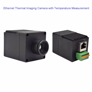


Thermal imaging camera module with dual output USB CVBS
This drone FPV thermal imaging camera supports both CVBS and USB video outputs.
1 Performance Parameters
| Thermal Model | Mini-640-CVBS | Mini-384-CVBS | Mini-256-CVBS | ||
| Detector Type | Vanadium oxide, uncooled, focal plane array detector | ||||
| Effective Pixels | 640 (H) ×512 (V) | 384 (H) ×288 (V) | 256 (H) ×192 (V) | ||
| Pixel Pitch | 12 μm | ||||
| Frame Rate (fps) | 50 | ||||
| Spectral Range | 8 μm–14 μm | ||||
| Net noise equivalent temperature difference (NETD) | ≤40mK@f/1.0 | ||||
| Physical Characteristics | |||||
| Focal Length (mm) | 9/13 | 9/13 | 4/7/10 | ||
| F1.0 | F1.0 | F1.0 | |||
| Field of view | 51.4° × 41.1°/32.9° × 26.6° | 28.7° × 21.7°/20.1° × 15.1° | 46.8°×34.1°/24.6°×18.59° /16.9°×12.8° | ||
| Dimension | 17.3 mm × 17.3 mm × 35.6 mm | ||||
| Net Weight (lens
excluded) |
21 g | ||||
| Image | |||||
| Brightness, Contrast, Sharpness
Adjustment |
Yes | ||||
| Gain Control | Auto/Manual | ||||
| Noise Reduction | 2D NR/3D NR | ||||
| Image Flip, Mirror | 180°/ Mirror | ||||
| Color Palettes | 18 (white hot/black hot/fusion/rainbow/golden autumn/midday/iron red/amber/jade/sunset/icefire/painting/pomegranate/
emerald/spring/summer/autumn/winter) |
||||
| Reticle | Display/Disappear/Hide | ||||
| Image Processing | UVC/Digital filtering noise reduction /Digital detail enhancement | ||||
| Interface | |||||
| Expansion Interfaces | CVBS /USB (2.0) | ||||
| Serial
Communication |
UART(3.3V)/USB serial interface | ||||
| Power | |||||
| Power Supply | 4.5–20 VDC | ||||
| Typical Power
Consumption@25℃ |
<0.75 W | <0.7 W | |||
| Environment | |||||
| Operating
Temperature |
–40 °C to +70 °C (–40 °F to +158 °F) | ||||
| Storage Temperature | –40 °C to +80 °C (–40 °F to +176 °F) | ||||
| Operating Humidity | 95% (no condensation) | ||||
| Vibrate | 6.06 g (0.01 lb), random vibration, all axial directions | ||||
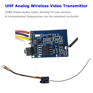
Mainboard Interfaces
CVBS Expansion Board
The CVBS expansion board supports two CVBS and USB interfaces, including a module power interface and Ca VBS analog video interface.
Mini-CVBS expansion board (mm [inch])

J2 :4-Pin USB interface
Table 3-2 Definition of J2 0.8T-WT-NP connector interface
| Pin No. | Pin Name | Type | Description |
| 1 | GND | Power | Grounded |
| 2 | USB_DP | Data positive signal | USB2.0 |
| 3 | USB_DM | Data negative signal | |
| 4 | +5 V | Power | Power input (5 VDC ± 10%) |
J3 :3-Pin CVBS interface
Table 3-3 Definition of J3 1.25T-7-LT-3A connector interface
| Pin No. | Pin Name | Type | Description |
| 1 | +4.5–20 V | Power | Power input (4.5–20 VDC) |
| 2 | GND | Grounded | |
| 3 | CVBS | Output | CVBS video signal |
J4:5-Pin CVBS interface
Table 3-4 Definition of J4 1.25T-1-LT-5A connector interface
| Pin No. | Pin Name | Type | Description |
| 1 | +4.5–20 V | Power | Power input (4.5–20 VDC) |
| 2 | GND | Grounded | |
| 3 | CVBS | Output | CVBS video signal |
| 4 | UART1_TXD_3V3 | Input/Output | Serial communication interface (3.3 V) |
| 5 | UART1_RXD_3V3 |


Video