


浅谈COFDM PA功率放大器
COFDM PA 功率放大器
作为无线视频和数据收发器的专业供应商, 很多客户会询问功率放大器,以增加无线发射器的覆盖范围,增强无线信号强度. 功放可以说是很多射频工程师无法回避的一道坎. 功能, 分类, 性能索引, 电路组成, 效率提升技术, 发展趋势... 关于射频功率放大器你需要知道的一切你都知道吗? 来补课吧!
RF PA 的两个关键规格: 功率和线性度
在射频功率放大器中, 功率效率 (佩) 定义为输出信号功率与输入信号功率之差与直流电源功耗的比值, 即:
PAE= (脉冲输出 - 普芬)/PDC= (脉冲输出 - 普芬)/(VDC*IDC)
射频功率放大器RF PA的功能
射频功率放大器RF PA是传输系统的主要部分, 其重要性不言而喻. 在发射机的前级电路中, 调制振荡电路产生的射频信号功率很小, 需要经过一系列的放大缓冲阶段, 中间放大阶段, 最后的功率放大级,在将辐射馈送到天线之前获得足够的射频功率. 为了获得足够大的射频输出功率, 必须使用射频功率放大器. 功率放大器通常是最昂贵的, 最耗电的, 以及固定装置或终端效率最低的组件.
调制器产生射频信号后, 射频调制信号被 RFPA 放大到足够的功率, 通过匹配网络, 然后由天线发射.
放大器的作用是将输入内容放大并输出. 输入和输出, 我们称之为 "信号," 通常表示为电压或功率. 为一个 "系统" 例如放大器, 它是 "贡献" 是为了提高某个水平 "吸收" 和 "产量" 对外界. 这个 "改进贡献" 是个 "意义" 放大器的存在. 如果功放能有好的性能, 那么它可以贡献更多, 反映了它自己的 "价值". 如果初期出现一些问题 "机构设计" 放大器的, 然后开始工作或工作一段时间后, 不仅无法提供任何 "贡献", 但有些出乎意料 "冲击" 可能会发生. "震惊" 对外界或放大器本身来说都是灾难性的.
射频功率放大器RF PA的分类
根据不同的工况条件, 功率放大器分类如下:
射频功率放大器的工作频率非常高, 但频段比较窄. 射频功率放大器一般采用选频网络作为负载电路. 射频功率放大器可分为三种工作状态: 一个 (一个), 乙 (乙), 和C (C) 根据电流导通角. A类放大器电流的导通角为360°, 适用于小信号低功率放大. B类放大器电流的导通角等于180°, C类放大器电流的导通角小于180°. B级和C级均适用于大功率工作条件, C类工况的输出功率和效率是三种工况中最高的. 大多数射频功率放大器工作在 C 类, 但C类放大器的电流波形失真太大, 因此它们只能通过使用调谐电路作为负载谐振来放大功率. 由于调谐环路的滤波能力, 环路电流和电压仍然接近正弦波形,失真很小.
除上述按电流导通角分类的工作状态外, 还有D类 (ð) 放大器和 E 类 (Ë) 使电子设备工作在开关状态的放大器. D类放大器的效率高于C类放大器.
射频功率放大器RF PA性能指标
射频功率放大器RF PA的主要技术指标是输出功率和效率. 如何提高输出功率和效率是射频功放设计目标的核心. 通常在射频功率放大器中, LC谐振电路可以选择基频或某个谐波,实现不失真放大. 一般来说, 评价放大器大概有以下几个指标:
- 获得. 这是输入和输出之间的比率,代表放大器的贡献. 一个好的放大器就是贡献尽可能多的 "产量" 尽可能在其范围内 "自身能力范围".
-工作频率. 这代表了放大器对于不同频率信号的承载能力.
- 工作带宽. 这决定了放大器的范围 "贡献". 对于窄带放大器, 即使自己的设计没有问题, 它的贡献可能是有限的.
-稳定. 每个晶体管都有潜力 "不稳定地区。" 该 "设计" 放大器需要消除这些潜在的不稳定性. 放大器稳定性有两种类型, 潜在不稳定和绝对稳定. 前者在某些条件和环境下可能会显得不稳定, 而后者在任何情况下都能保证稳定性. 稳定性问题很重要,因为不稳定意味着 "振荡", 当放大器不仅影响其自身时, 但也输出不稳定因素.
- 最大输出功率. 该指标决定了 "容量" 放大器的. 对于 "大系统", 希望以牺牲一定的增益为代价,输出更大的功率.
-效率. 放大器必须消耗一定量的 "活力" 并且还达到了一定的数量 "贡献". 其对功耗的贡献之比就是放大器的效率. 好的放大器是贡献多、消耗少的放大器.
- 线性. 线性度表征放大器对大量输入的正确响应. 线性度恶化意味着放大器 "扭曲" 要么 "扭曲" 存在过量输入时的输入. 好的放大器不应该表现出这种情况 "怪异的" 自然.
射频功率放大器RF PA的电路组成
有不同类型的放大器. 简, 放大器电路可由以下部分组成: 晶体管, 偏置和稳定电路, 以及输入输出匹配电路.
1. 晶体管
晶体管有很多种, 包括已发明的各种结构的晶体管. 本质上, 晶体管通过将空直流电的能量转换为受控电流或电压源来工作 "有用" 产量. 从外界获取直流能量, 晶体管消耗它并将其转换成有用的组件. 晶体管, 我们可以把它看作 "一个单位". 不同的 "能力" 不同晶体管的, 比如他们承受力量的能力不同, 这也是由于它们能够获得直流能量; 例如, 他们的反应速度不同, 这决定了它可以工作的频段有多宽和多高; 例如, 输入端和输出端面对的阻抗不同, 以及对外的响应能力不同, 这决定了匹配的难度.
2. 偏置和稳定电路
偏置和稳定电路是两个不同的电路, 但因为它们往往难以区分并且设计目标趋同, 他们可以一起讨论.
晶体管的工作需要在一定的偏置条件下, 我们称之为静态工作点. 这是晶体管及其自身的基础 "定位". 每个晶体管都有一定的自身定位, 而不同的定位会决定自己的工作模式, 并且在不同的定位上也有不同的表现. 部分定位点波动较小, 适合小信号工作; 部分定位点波动较大, 适合大功率输出; 部分定位点需求较少, 纯粹的释放, 适合低噪音工作; 一些定位点, 晶体管总是在饱和和截止之间徘徊, 处于切换状态. 合适的偏置点是正常工作的基础.
稳定电路必须位于匹配电路之前, 因为晶体管需要稳定电路作为其本身的一部分, 然后联系外界. 在外界眼中, 具有稳定电路的晶体管是 "全新" 晶体管. 它使得确定 "牺牲" 获得稳定. 稳定电路的机制使晶体管保持平稳运行.
3. 输入输出匹配电路
匹配电路的目的是选择可接受的模式. 对于那些想要提供更多增益的晶体管, 方法是全面接受并输出. 这意味着通过匹配电路的接口, 不同晶体管之间的通讯更加顺畅. 适用于不同类型的放大器, 匹配电路并不是唯一的设计方法 "完全接受". 一些直流小、基础浅的小管在接收时更愿意做一定量的遮挡,以获得更好的噪声性能. 然而, 封锁不能过度, 否则会影响其贡献. 对于一些巨型功率管, 输出时需要谨慎, 因为它们更不稳定, 同时, 一定量的保留可以帮助他们发挥更多的作用 "不失真的" 活力.
射频功率放大器RF PA稳定性的实现
每个晶体管都可能不稳定. 好的稳定电路可以与晶体管熔合,形成一个 "连续工作" 模式. 稳定电路的实现可分为两种类型: 窄带和宽带.
窄带稳定电路消耗一定的增益. 该稳定电路是通过增加一定的消耗电路和选择电路来实现的. 该电路允许晶体管仅贡献很小的频率范围. 另一种宽带稳定性是引入负反馈. 该电路可以在很宽的范围内工作.
不稳定的根源是正反馈, 窄带稳定性的思想是抑制一些正反馈. 当然, 这也抑制了贡献. 负面反馈, 做得好, 还有许多额外的令人欣喜的优点. 例如, 负反馈可能会阻止晶体管匹配, 无需匹配即可与外界良好交互. 此外, 负反馈的引入将改善晶体管的线性性能.
射频功率放大器RF PA效率提升技术
晶体管效率有理论极限. 该限制随偏置点的选择而变化 (静态工作点). 此外, 如果外围电路设计不好, 它的效率将会大大降低. 现在, 工程师提高效率的方法并不多. 这里只有两种: 包络跟踪技术和Doherty技术.
包络跟踪技术的本质是将输入分为两类: 相位和包络线, 然后通过不同的放大电路分别放大. 这样, 两个放大器可以专注于各自的部分, 两个放大器的配合可以达到更高效率利用的目的.
Doherty技术的本质是: 使用两个相同类型的晶体管, 当输入很小时只有一个有效, 并处于高效率状态. 如果输入增加, 两个晶体管同时工作. 这种方法实现的基础是两个晶体管要默契地配合. 一个晶体管的工作状态将直接决定另一个晶体管的工作效率.
RF PA 的测试挑战
功率放大器是无线通信系统中非常重要的组件, 但它们本质上是非线性的, 引起干扰相邻通道的光谱增长现象, 并可能违反法定带外发射标准. 该特性甚至会导致带内失真, 这会增加误码率 (BER) 并降低了通信系统的数据传输速率.
峰均功率比下 (辣椒), 新的 OFDM 传输格式将具有更多零星峰值功率, 使得 PA 难以分段. 这会降低频谱模板合规性并增加整个波形的 EVM 和 BER. 为了解决这个问题, 设计工程师通常会刻意降低PA的工作功率. 很遗憾, 这是一种非常低效的方法, 由于 PA 减少 10% 其经营能力并失去 90% 其直流电源.
当今大多数 RF PA 支持多种模式, 频率范围, 和调制模式, 提供更多测试项目. 上千个测试项目并不少见. 使用波峰因数降低等新技术 (CFR), 数字预失真 (DPD) 和包络跟踪 (ET) 有助于优化 PA 性能和电源效率, 但这些技术只会让测试变得更加复杂并大大延长测试时间. 设计及测试时间. 增加 RF PA 的带宽将导致 DPD 测量所需的带宽增加五倍 (可能超过 1 千兆赫), 进一步增加测试复杂性.
按照趋势, 为了提高效率, RF PA 组件和前端模块 (有限元法) 将更加紧密地结合在一起, 单个 FEM 将支持更广泛的频段和调制模式. 将 ET 电源或调制器集成到 FEM 中可以有效减少移动设备内部的整体空间需求. 增加滤波器/双工器插槽数量以支持更大的工作频率范围将增加移动设备的复杂性和测试项目的数量.
手机射频模块功放 (PA) 市场情况
手机功放领域目前是手机中无法集成的元件. 手机性能, 脚印, 通话质量, 手机实力, 和电池寿命都是由功放决定的.
如何将这些不同频段、不同标准的功放集成起来,是业界一直在研究的重要课题. 目前, 有两种解决方案: 一是融合架构, 集成了不同频率的射频功率放大器PA; 另一种架构是沿信号链的集成, 那是, PA和双工器集成在一起. 两种方案各有优缺点, 并且适用于不同的手机. 融合架构, PA高度集成, 规模优势明显 3 频带, 以及明显的成本优势 5-7 频带. 缺点是虽然PA是集成的, 双工器还是相当复杂的, PA集成时存在开关损耗, 并且性能会受到影响. 对于后一种架构, 性能更好. 功率放大器和双工器的集成可以改善电流特性, 可节省数十毫安电流, 这相当于延长通话时间 15%. 因此, 业内人士建议,当超过 6 频带 (不包括2G, 指的是3G和4G), 采用融合架构, 并且当小于 4 使用频段, 软垫, PA和双工器集成的解决方案, 被使用.
-
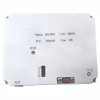
 高压宽带功率运算放大器模块, 50电压峰值1A, 直流-1MHz, 稳定的容性负载驱动器
-
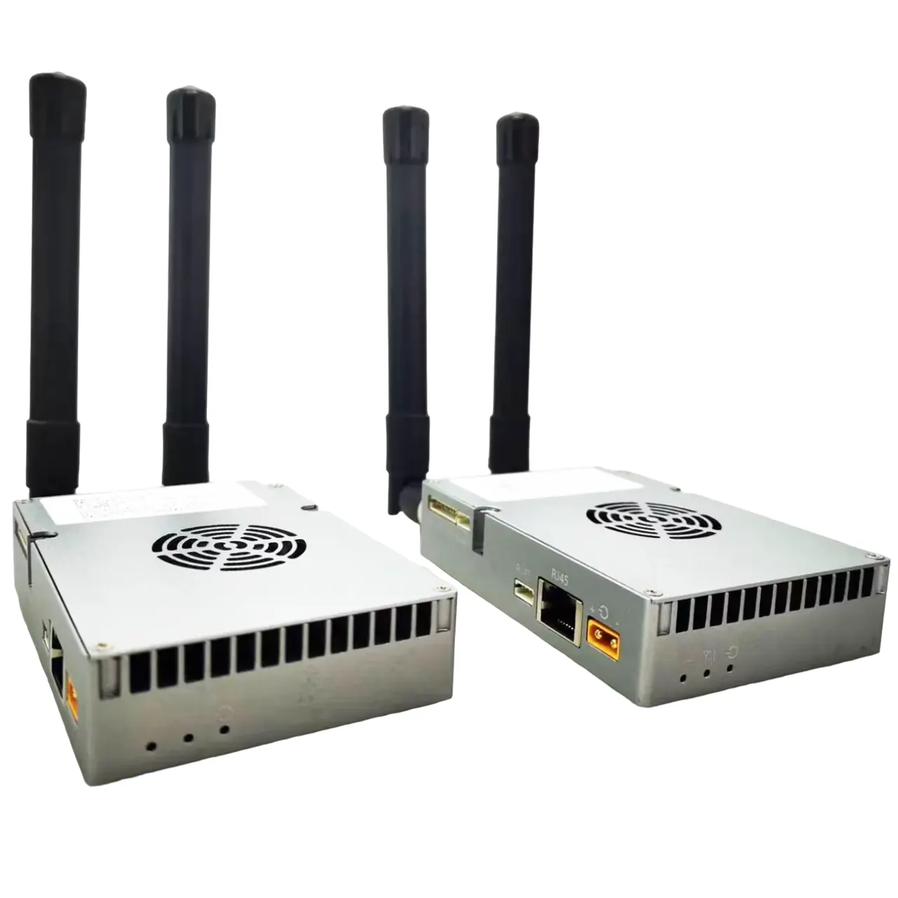
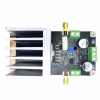
 带 PA 的 L 频段 2W TDD 射频前端模块, LNA 和高速 T/R 开关 (1100–1500 MHz)
价格范围:$336.00 至 $460.00
带 PA 的 L 频段 2W TDD 射频前端模块, LNA 和高速 T/R 开关 (1100–1500 MHz)
价格范围:$336.00 至 $460.00 -
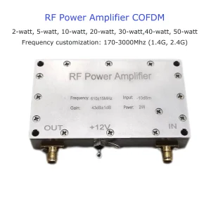
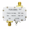 射频功率放大器 2 瓦 200MHz 发射放大器模块
-
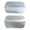
 2T2R TDD-1420-1530-2×5W射频功放模块
价格范围:$480.00 至 $690.00
2T2R TDD-1420-1530-2×5W射频功放模块
价格范围:$480.00 至 $690.00 -
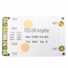 TDD 2T2R功放模块1100-1500MHz | 1300M 2W 5W 10W 30W RF PA 射频前端模块
价格范围:$460.00 至 $998.00
TDD 2T2R功放模块1100-1500MHz | 1300M 2W 5W 10W 30W RF PA 射频前端模块
价格范围:$460.00 至 $998.00 -
 FDD射频放大器
原价为:$2,500.00。$950.00当前价格为:$950.00。
FDD射频放大器
原价为:$2,500.00。$950.00当前价格为:$950.00。 -
 20WPA 2.4G 5.8G 功率放大器 无人机数据链信号增强器
价格范围:$169.00 至 $269.00
20WPA 2.4G 5.8G 功率放大器 无人机数据链信号增强器
价格范围:$169.00 至 $269.00 -
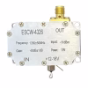 1WPA 1瓦功率放大器ESCW-4326 MCX SMA RF 12-18V 1300-1400MHz
$192.00
1WPA 1瓦功率放大器ESCW-4326 MCX SMA RF 12-18V 1300-1400MHz
$192.00