
This document provides a comprehensive technical overview of the CX660X series broadband wireless data transmission module, a high-performance communication module designed for long-range, low-latency data and video transmission. The CX660X module is based on LTE wireless communication technology and integrates advanced technologies such as OFDM (Orthogonal Frequency Division Multiplexing) そして MIMO (Multiple-Input Multiple-Output) to deliver stable, high-throughput wireless links in complex environments.
The manual begins with a clear explanation of the module usage and system integration, including detailed data transmission and command transmission workflows. It describes how the CX660X operates as the core communication unit in a wireless video or data link system, interfacing with host controllers through USB, HSIC, and UART interfaces. These sections help developers and system integrators quickly understand how to connect cameras, processors, and control units to achieve reliable uplink and downlink communication.
A major portion of the document is dedicated to the functional features and performance specifications of the CX660X. It outlines supported RF frequency bands, 含む 800 メガヘルツ, 1.4 GHz, そして 2.4 GHz, as well as flexible bandwidth options ranging from 1.4 MHzから 20 メガヘルツ. The document also provides in-depth information on transmit power, 受信感度, modulation schemes, data rates, and network capacity, demonstrating the module’s suitability for both short-range and ultra-long-range transmission scenarios.
The technical manual further includes electrical characteristics, mechanical dimensions, power consumption profiles, and low-power operating modes, enabling engineers to accurately evaluate power budgets and thermal performance. Detailed PIN definitions and interface descriptions are provided to support hardware design, PCB integration, and system debugging.
加えて, the document covers system reliability, environmental specifications, EMC compliance, and regulatory considerations, such as RoHS and REACH requirements. These sections highlight the CX660X module’s readiness for industrial-grade applications.
全体, this document serves as a complete reference for developers working on UAV data links, ワイヤレスビデオ伝送システム, 遠隔監視, and industrial communication equipment. It offers both high-level system understanding and low-level hardware details, making it an essential guide for product development, 統合, and deployment of CX660X-based wireless solutions.
CX660X Module Product Technical Manual
CX660X Module Product Technical Manual
- CX660X Module Usage
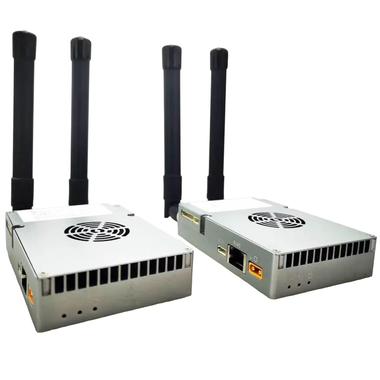
The CX660X is a point-to-multipoint broadband data transmission module. Based on the LTE wireless communication standard, it utilizes key technologies such as OFDM (Orthogonal Frequency Division Multiplexing) and MIMO (Multi-Input & Multi-Output). The module supports multiple bandwidth allocations (1.4メガヘルツ, 3メガヘルツ, 5メガヘルツ, 10メガヘルツ, and 20MHz) and features a flat system architecture design, effectively reducing system latency and improving transmission capability. It offers long-range transmission, high data throughput, and strong anti-interference performance. Equipped with an SOC chip, the CX660X achieves higher integration, significantly reduces system power consumption, and minimizes module size, making it ideal for customer applications such as UAVs and video surveillance systems.

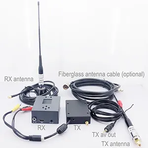
CX660X As the communication component of the image transmission system, 送信機…/The data is received from the main control module, and the specific data flow is as follows:
- Data sending and receiving process
| 送信 | The main control module is an image acquisition device that performs data acquisition and encoding. | カメラ |
| The main control module transmits the encoded data to the CX660X via a USB or HSIC interface. | Physical interface: USB/HISC; Logically virtual:Network card | |
| The CX660X transmits the received encoded image data to [the target device] via the air interface.receiver | ||
| take over | The receiver CX660X receives the encoded image data and passes it through to the main controller.Module | |
| The CX660X transmits data to the main control module via USB or HSIC interface. | Physical interface: USB/HISC; Logically virtual:Network card | |
| After receiving data from the CX660X, the main control module performs image decoding and display. |
- Command sending and receiving process
| 送信 | The main control module sends control commands to the CX660X via the UART interface. | |
| The CX660X transmits the received control data to the receiving end via the air interface. | Data and instructions are separated at the hardware interface. | |
| take over | The receiving end CX660X receives control data and transmits it to the main controller via UART.Manufacturing module |
- CX660X Module Functions and Performance Specifications
| 機能 | Functional description | detailed | 述べる |
| PCB area | 43.40mm*45.00mm*3.00mm (Single-sided PCB) | Tolerance range: 43.40±0.15mm 45.00±0.15mm 3.00±0.10mm | |
| RF | Radio frequency band | 2401.5-2481.5 メガヘルツ 1427.9-1447.9メガヘルツ 806-826 メガヘルツ | |
| 力, etc.class | 2.4G/1.4G/800M 25dBm±2 | ||
感度(Access) | 2.4G (channel number 24415): 20メガヘルツ -99 10メガヘルツ -103 5メガヘルツ -104 3メガヘルツ -106 | Access status | |
| 1.4G (channel number 14379) 10メガヘルツ -103 5メガヘルツ -104 3メガヘルツ -106 | Access status | ||
| 800M (channel number 8160) 10メガヘルツ -103 5メガヘルツ -104 3メガヘルツ -106 | Access status | ||
Sensitivity( BLEY<=3%) | 2.4G(24415 (周波数): 20MHz -94dBm(10Mbpsの) 20MHz -97dBm(5Mbpsの) 10MHz -91dBm(10Mbpsの) 10MHz -96dBm(5Mbpsの) 5MHz -84dBm(10Mbpsの) 5MHz -93dBm(5Mbpsの) 3MHz -87dBm(5Mbpsの) 3MHz -98dBm(2Mbpsの) 2MHz -84dBm(2Mbpsの) | ||
| 1.4G(14379 (Frequency point) 10MHz -91dBm(10Mbpsの) 10MHz -96dBm(5Mbpsの) 5MHz -82dBm(10Mbpsの) 5MHz -91dBm(5Mbpsの) 3MHz -86dBm(5Mbpsの) 3MHz -97dBm(2Mbpsの) 2MHz -84dBm(2Mbpsの) | |||
| 800M(8160 (周波数): 10MHz -91dBm(10Mbpsの) 10MHz -97dBm(5Mbpsの) 5MHz -84dBm(10Mbpsの) 5MHz -94dBm(5Mbpsの) 3MHz -87dBm(5Mbpsの) 3MHz -98dBm(2Mbpsの) 2MHz -84dBm(2Mbpsの) |
| 2MHz -84dBm(2Mbpsの) | |||
| インタフェース | UART | 2 indivual | |
| HSIC | USB 2.0 高速 | ||
| USB | USB 2.0 高速 | ||
| I2C | 1 indivual | ||
| GPIO | 6 indivual | ||
| JTAG | 1 indivual | ||
| アンテナ | デュアルアンテナ | ||
| 電源 | VBAT | 3.7V~4.35V; | 入力 |
| D1V8A | External power supply interface | 出力 | |
| D2V85A | JTAG、センサー、2.85V External power supply interfacesource | 出力 | |
| VCC_HSI C2LAN | Reserved for externalLAN9730Chip power supply,3.3V | 出力 | |
| Transmission method | Unicast, マルチキャスト, 放送 | サポート | |
| Power control | 自動電力制御 | Support adaptive control | |
| Fixed power | サポート | ||
| ソフトウェアのアップグレード | OTA | Supports OTA (Over-The-Air) updates, and supports both local and remote upgrades. | |
| Configuration Management | WEB UI | Meets basic configuration requirements / 報告 / Query function | |
| 干渉防止 | dynamic frequency tuning | Supports cross-band frequency hopping | |
| Retransmission configuration | HARQ Retransmission | サポート | |
Transmission mode | Transmission Module Mode | Single antenna for transmitting, single antenna for receiving / single antenna Transmit, dual-antenna reception | |
| Data Link | Master-slave bidirectional data communication | ||
| uplink and downlink Ratio | The central node supports configurable uplink and downlink time-slot ratios: 2D3U / 3D2U / 4D1U / 1D4U | ||
動作帯域幅 | 2.4GHz | 1.4メガヘルツ / 3メガヘルツ / 5メガヘルツ / 10メガヘルツ / 20メガヘルツ | |
| 1.4GHz | 1.4メガヘルツ / 3メガヘルツ / 5メガヘルツ / 10メガヘルツ / 20メガヘルツ | ||
| 800メガヘルツ | 1.4メガヘルツ / 3メガヘルツ / 5メガヘルツ / 10メガヘルツ / 20メガヘルツ | ||
データレート | Peak Throughput | A single node supports up to 30 Mbpsの in one direction, そして最大まで 45 Mbpsの bidirectionally. | |
| Rate Levels | Adaptive average disSystem throughput is adaptively and evenly allocated among nodes. | ||
| Speed limit | Supports user speed User-configurable bandwidth limiting is supported | ||
| 暗号化 | ZUC,SNOW3G,AES Three types of encryption Option | ||
| modulationWay | QPSKをサポート, 16QAM, and 64QAM modulation schemes. |
| Supported Number of Network Nodes | Supports a network size of N ≥ 2, with up to 16 アクセスノード. | ||
| DRX | Master node controls, slave nodes allow entry DRX 160ms cycle | ||
| 伝送距離 | Service video transmission distance | Support 0-3Km | CX6601 / CX6601N (No external PA switching interface) |
| Support 0-10Km | CX6602 / CX6602N (No external PA switching interface) | ||
| Supports 0-30Km | CX6603 | ||
| Support Ultra-long distance 0 – 80Km | CX6608 | ||
| Support Ultra-long distance 0 – 150Km | CX6609 | ||
| 遅れ | Air interface latency | From node- Central node transmission delay<=200ms | USB/HSIC data transmission |
| Module air interface delay | UL One-way, delay<20ms DL One-way, delay<20ミズ | CFG0 1V4 DRX Disabled | |
| Power-On Delay | Central Node/ The node boot latency is less than15s | ||
| System Control | Parameter Configuration | 送信電力 / 周波数 / 帯域幅 (Real-time Adjustable), 周波数帯域 (Non-Real-time Adjustable) | |
| 状態 / Parameter Reporting | Connection Status / RSRP / SNR / 距離 / Uplink & Downlink Throughput, 等. | ||
| OTG interface | OTG | Module USB Interface for connecting external devices | Physical interface: USB |
Transmitter spurious | <-36dBm @BW=1kHz | 9KHz=< f < 150KHz | |
| <-36dBm @BW=10kHz | 150KHz=< f < 30メガヘルツ | ||
| <-36dBm@BW=100kHz | 30MHz=< f < 1000メガヘルツ |
| <-36dBm @BW=1MHz | 1GHz=< f < 12.75GHz | ||
| Uplink EVM | <6% | ||
| ACLR | <-29.2dBc@E-UTRA1 <-32.2dBc@UTRA1 <-35.2dBc@UTRA2 | ||
| 消費電力 | peak | Power Consumption at Maximum Data Rate: 700 mA ±15% | |
Low power mode | Controlled by AT | AT Command-Controlled Low Power Mode: Allows wake-up via short press of the power button or by network activity. Standby without active connections: ≤ 60 mA Soft shutdown state: ≤ 10 mA | |
| モジュール重量 | Standard board | 13 グラム |
- ハードウェア ピン Pin definitions:
| Tubefoot | ピン名 | Voltage domain | IO | Function Description | 述べる |
| 1 | GND | 土地 | |||
| 2 | HSIC_DATA | IO | HSIC Data cable | ||
| 3 | GND | 土地 | |||
| 4 | HSIC_STROBE | IO | HSIC strobe signal | ||
| 5 | GND | 土地 | |||
| 6 | UART0_RX | 1.8V | 私 | serial port0 Receiving | |
| 7 | UART0_TX | 1.8V | ○ | serial port0 Send | |
8 | RSTIN_N | 1.8V | 私 | Module system reset input, active low.Greater than32ms | |
| 9 | GND | 土地 | |||
| 10 | GPIO3 | 1.8V | IO | GPIO | Link establishment indicator – blue light |
11 | GPIO0 | 1.8V | IO | GPIO | AMT Detection: AMT mode is triggered when the signal is high (another method—fixture shorting GPIO0/3—also triggers AMT, omitted here). Low signal indicates normal startup. |
12 | GPIO2 | 1.8V | IO | GPIO | DUMP Indicator: Physical layer dump; red LED lights up. |
13 | GPIO1 | 1.8V | IO | GPIO | Link Establishment Indicator: Goes high when the link is successfully established; green LED lights up. |
| 14 | GPIO4 | 1.8V | IO | GPIO | Restore System Defaults: Default state is high; pull low to reset. |
| 15 | GPIO5 | 1.8V | IO | GPIO | Default Low Level: When low, USB is used as the command interface; When high, UART is used as the command interface. |
| 16 | UART0_CTS | 1.8V | 私 | UART0_CTS | |
| 17 | UART0_RTS | 1.8V | ○ | UART0_RTS | |
| 18 | GND | 土地 | |||
| 19 | COMUART_RX | 2.85V | 私 | COMUARTreceive | Compatible 3.3V interface |
| 20 | COMUART_TX | 2.85V | ○ | COMUARThair | Compatible 3.3V interface |
| 21 | GND | 土地 | |||
| 22 | GND | 土地 | |||
| 23 | GND | 土地 | |||
| 24 | PRIMARY_ANT | IO | Main transceiver antenna | ||
| 25 | GND | 土地 | |||
| 26 | GND | 土地 | |||
| 27 | SECONDARY_ANT | 私 | Auxiliary receiving antenna | ||
| 28 | GND | 土地 | |||
| 29 | GND | 土地 | |||
| 30 | GND | 土地 | |||
| 31 | GND | 土地 | |||
| 32 | GND | 土地 | |||
33 | VCC_HSIC2LAN | 3.3V | ○ | Provides 3.3 V Power to External HSIC-to-LAN Chip | |
| 34 | GND | 土地 | |||
| 35 | JTAG_TDI | 2.85V | 私 | JTAG Signal | |
| 36 | JTAG_NTRS | 2.85V | 私 | JTAG Signal | Planned for OTG Functionality: Default state is high; pull low to activate. |
| 37 | JTAG_TMS | 2.85V | 私 | JTAG Signal | |
| 38 | JTAG_TDO | 2.85V | ○ | JTAG Signal | |
| 39 | JTAG_TCK | 2.85V | 私 | JTAG Signal | |
40 | TMODE0 | 2.85V | 私 | 低い: Trace Coresight 高い: Trace X1643 + XC4210 + TL420 | |
| 41 | D2V85 | 2.85V | ○ | 2.85V Interface electricity,JTAG Interface power | |
| 42 | GND | 土地 | |||
| 43 | VSB | 3V | 私 | RTC Battery powered | |
| 44 | D1V8 | 1.8V | ○ | 1.8VInterface power | |
| 45 | GND | 土地 | |||
| 46 | GND | 土地 | |||
| 47 | VCC | VCC | 私 | Main power supply,3.7V~4.35V | |
| 48 | VCC | VCC | 私 | Main power supply | |
| 49 | VCC | VCC | 私 | Main power supply | |
| 50 | GND | 土地 | |||
| 51 | GND | 土地 | |||
| 52 | GND | 土地 | |||
| 53 | POWER_KEY | 1.8V~VBAT | 私 | Power-On Signal: Active high |
54 | DL | 1.8V | 私 | Download Key: Hold high to initiate download. | Power-On/Download Button: Active high. When downloading software, POWER_KEY must be held low. |
| 55 | I2C_SCL | 1.8V | ○ | I2C clock signal | |
| 56 | I2C_SDA | 1.8V | IO | I2C Clock data | |
| 57 | GND | GND | |||
| 58 | ノースカロライナ州 | ||||
| 59 | ノースカロライナ州 | ||||
| 60 | ノースカロライナ州 | ||||
| 61 | ノースカロライナ州 | ||||
| 62 | ノースカロライナ州 | ||||
| 63 | ノースカロライナ州 | ||||
| 64 | ノースカロライナ州 | ||||
| 65 | ノースカロライナ州 | ||||
| 66 | ノースカロライナ州 | ||||
| 67 | ノースカロライナ州 | ||||
| 68 | GND | GND | |||
| 69 | USB0_DP | IO | USB Differential Signal | ||
| 70 | USB0_DM | IO | USB Differential Signal | ||
| 71 | GND | GND |
- Electrical characteristics
| PARAMETER | SYMBOL | 説明 | MIN | TYPE | マックス | UNIT |
| System main power supply | VCC | 入力 | 3.7 | 3.8 | 4.35 | で |
| External power supply interface | D1V8 | 出力 | 1.8 | で | ||
| External power supply interface | D2V85 | 出力 | 2.85 | で | ||
| RTC Battery powered | VSB | 入力 | 3 | で |
- Mechanical parameters


- CX660X General Description
- 保護/Safety regulations/Environmental Specifications
| Sub-requirement name | 説明する |
| EMC | satisfy 3GPP TS34.124 Standard requirements |
- Environmental protection specifications
| Sub-requirement name | 説明する |
| RoHSRequire | Meets China RoHS requirements |
| REACH | Meets China REACH 2009 要件 |
| Halogen Free | Meets International Electrotechnical Commission (IEC) 標準 61249-2-21:2003 |
述べる:
RoHS is a universally accepted requirement both domestically and internationally.
REACH is a requirement of the European Union, and imported products in China must also meet this requirement; Halogen Free is a requirement of the European Union.
- 外観

- MSD grade
3(Moisture-sensitive devices).
- Reliability indicators
| Sub-item name | 説明する |
温度範囲 | 動作温度:-20°C~75°CStorage temperature:-40°C~85°C |
| 湿度 | 5%~95% |
ESD | all pin touch ±1KV |
| Antennapin touch ±4 kW | |
| Antennapin space ±8KV |
質問する
ご回答をありがとうございました。 ✨